The Diode Clock
April 2025 - Present
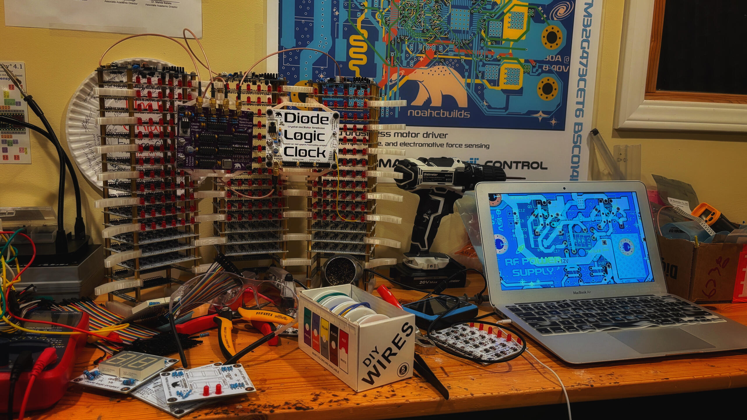
The Diode Clock is a 24-hour clock that uses diodes instead of transistors for logic and display functions. The clock was designed by Teddy Yapo from 2012 to 2016, and he documented the project on Hackaday. I remade Yapo's clock with some additions and redesigns.In diode logic, a diode OR gate pairs with a diode-based inverter to form a NOR gate. NOR gates are capable of implementing all Boolean functions.The clock contains radio-frequency (RF) power supplies, diode logic gates, diode encoders, a spectrum generator, and a crystal oscillator timebase. The power supplies, spectrum generator, and timebase use transistors and ICs. 62 PCBs distribute 6000+ total components.As transistor scaling slows, alternative computing methods become more important. Diode logic won’t replace transistor-based TTL or CMOS. But I’ve had fun and learned a lot exploring its quirks.
1. Diode Clock Logic Board
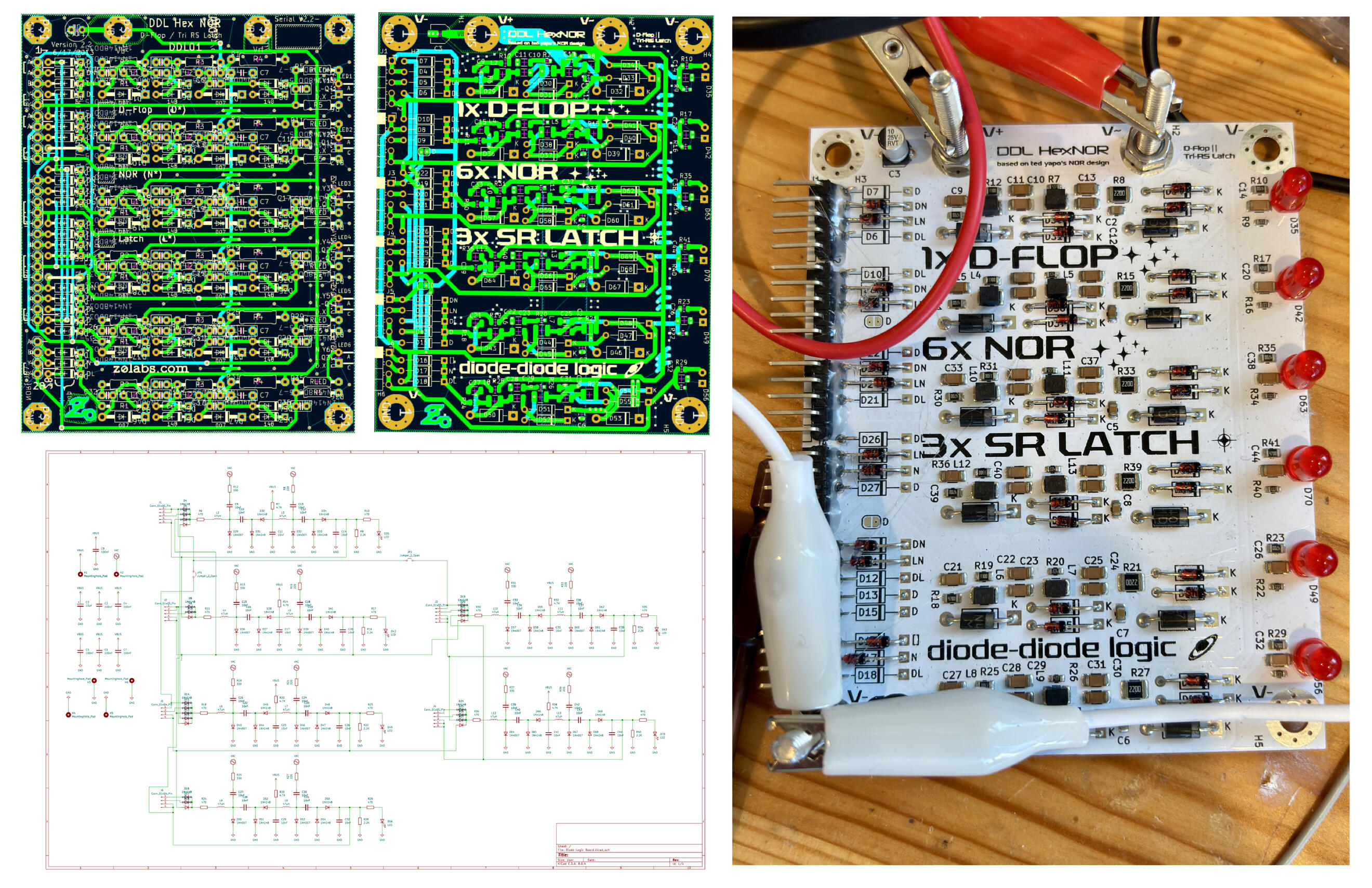
After building TenniBear, I wanted to work on something purely electronic. While browsing Hackaday, I found Ted Yapo’s Diode Clock. The clock stood out to me for the wide range of electronics involved and the complexity. I predicted building the clock would keep me occupied for months and teach me more about electrical engineering. After a few days of poring over Yapo's project logs, I committed to building his clock with some redesigns.The clock is built around diode logic boards (mine uses 48, while Yapo’s uses 46, for reasons I’ll show later). The top left is design is his. To the right is mine, with fewer through-hole components and thicker traces. Manual assembly/soldering time was reduced from around 1 hour/board (for Yapo’s design) to 15 minutes. Using JLCPCB instead of OSH Park (Yapo's supplier) reduced prices from $20/board to $4/board.The board consists of six NOR gates each made of diodes, capacitors, resistors, and inductors. The board is reconfigurable as a data flip flop or 3 set-reset latches. The red LEDs display output state. Powered with 5V DC and 12Vp-p RF supplied by custom power supply (next slide).
~Redesigned April 2025, finished assembly August
2. Diode Clock Radio-Frequency Power Supply Board
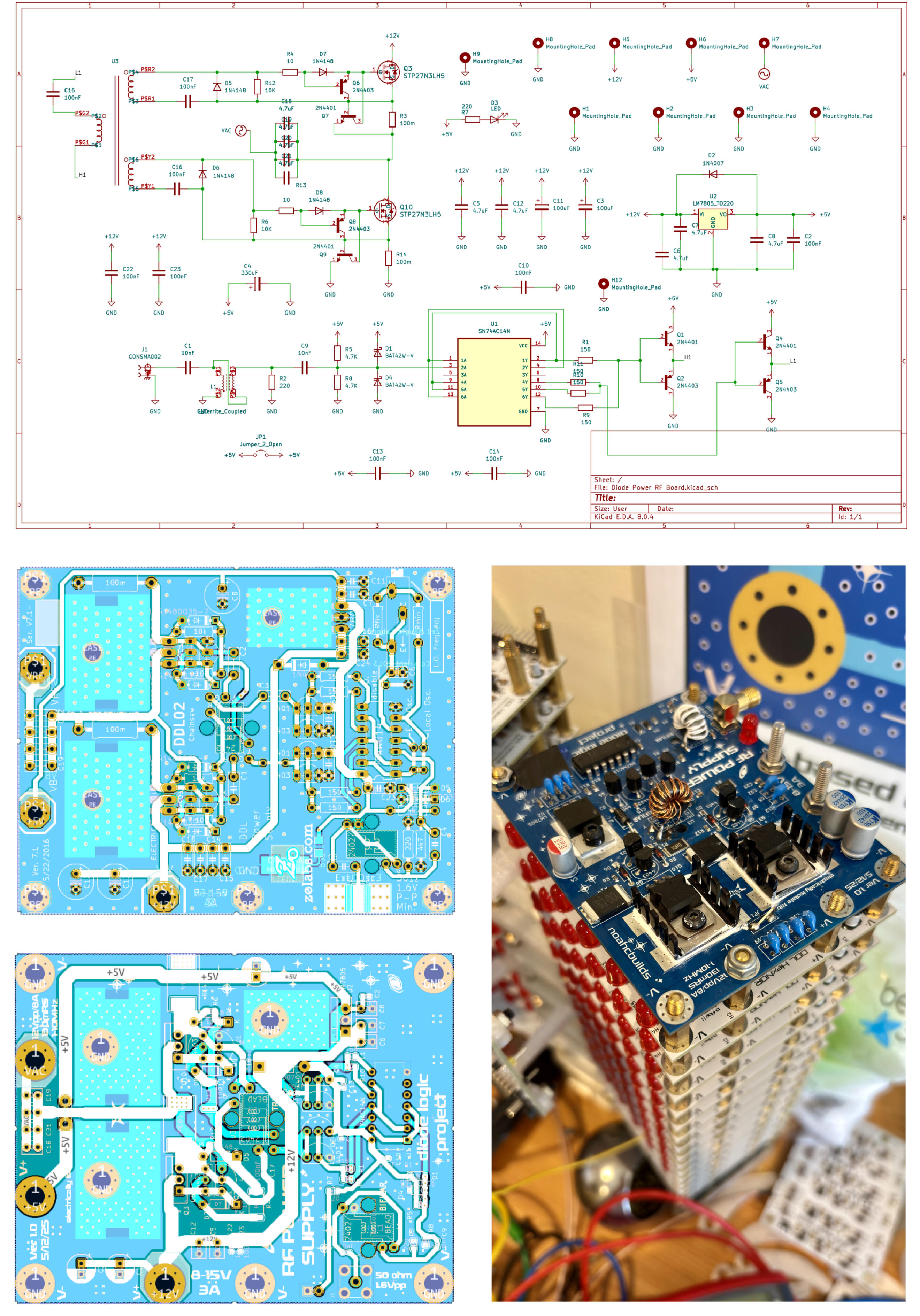
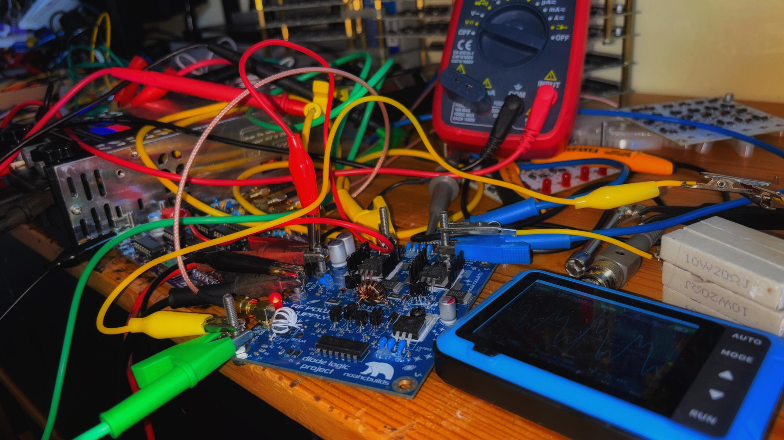
Yapo’s diode logic NOR gates require an RF power source (middle left), which allows for signal inversion (DC bias from inputs inversely determining whether RF current is shunted to ground via diodes, resulting in a low output, or blocked and allowed to continue, producing a high output). Bottom left is my redesign, with the local oscillator section removed. Crucially, the aluminum organic polymer caps Yapo used for input noise filtering were no longer manufactured. I found my own with similar equivalent series resistance (ESR) and ripple current values. I also increased the power rating of the current-limiting resistors (R3 and R14 in schematic).Assembly of the switching MOSFETs was delicate, with layers of insulation, thermal grease, and heatsinks. Bottom right is a picture of an assembled power supply on top of a stack of logic boards. Three of these “logic stacks” make up my version of the clock.
~Redesigned April 2025, finished assembly August
3. Diode Clock Divisor, Spread Spectrum Generator, 7-Segment Diode Encoder
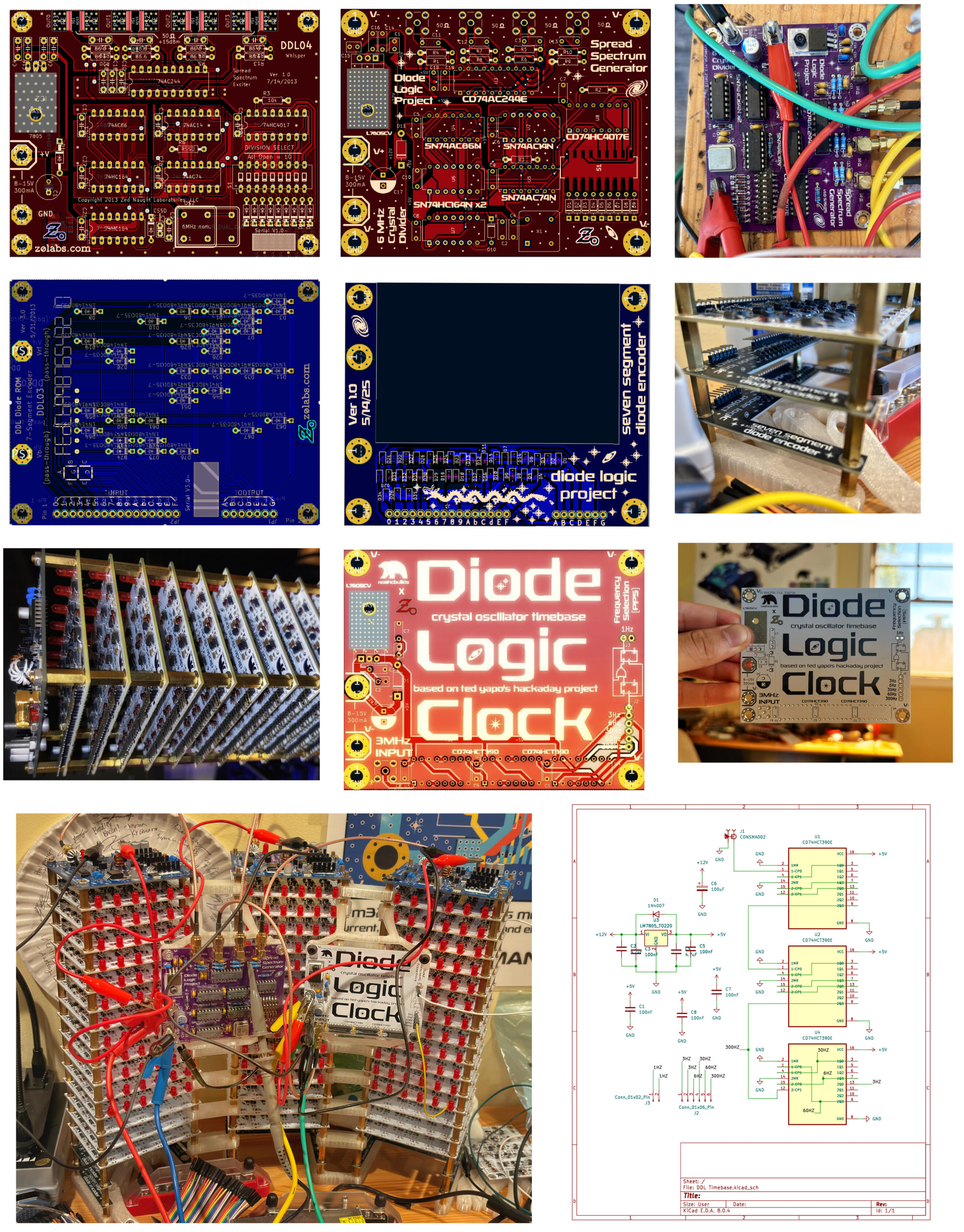
Top pictures depict the external oscillator used for the power supply input signals. I kept this board mostly identical to Yapo’s, except for some footprints (SMA jack, crystal). The board provides 3 MHz signals to 4 RF power supplies, reducing EMI by keeping them in opposite phases. I condensed my clock to 3 power supplies which reduced the anti-EMI effectiveness, but I compensate using an RC snubber across the supply outputs.Below the spectrum generator is a diode encoder for 7-segment displays (the display boards I have yet to make). The bright red board is my self-designed timebase, dividing the 4th output of the spectrum generator (3 MHz) down to 1 Hz (clock source). I chained three 4-bit decade counter ICs in series to get from 3 MHz to 3 Hz. To get from 3 Hz to 1 Hz, I use two D flip flops and an extra NOR gate (reason for needing 48 logic boards instead of 46). Bottom right is the schematic of the timebase, and bottom left are my three “logic stacks” with the spectrum generator and timebase.
~Redesigned May 2025, finished assembly August
4. Diode Clock Power Supply + Logic Board Testing
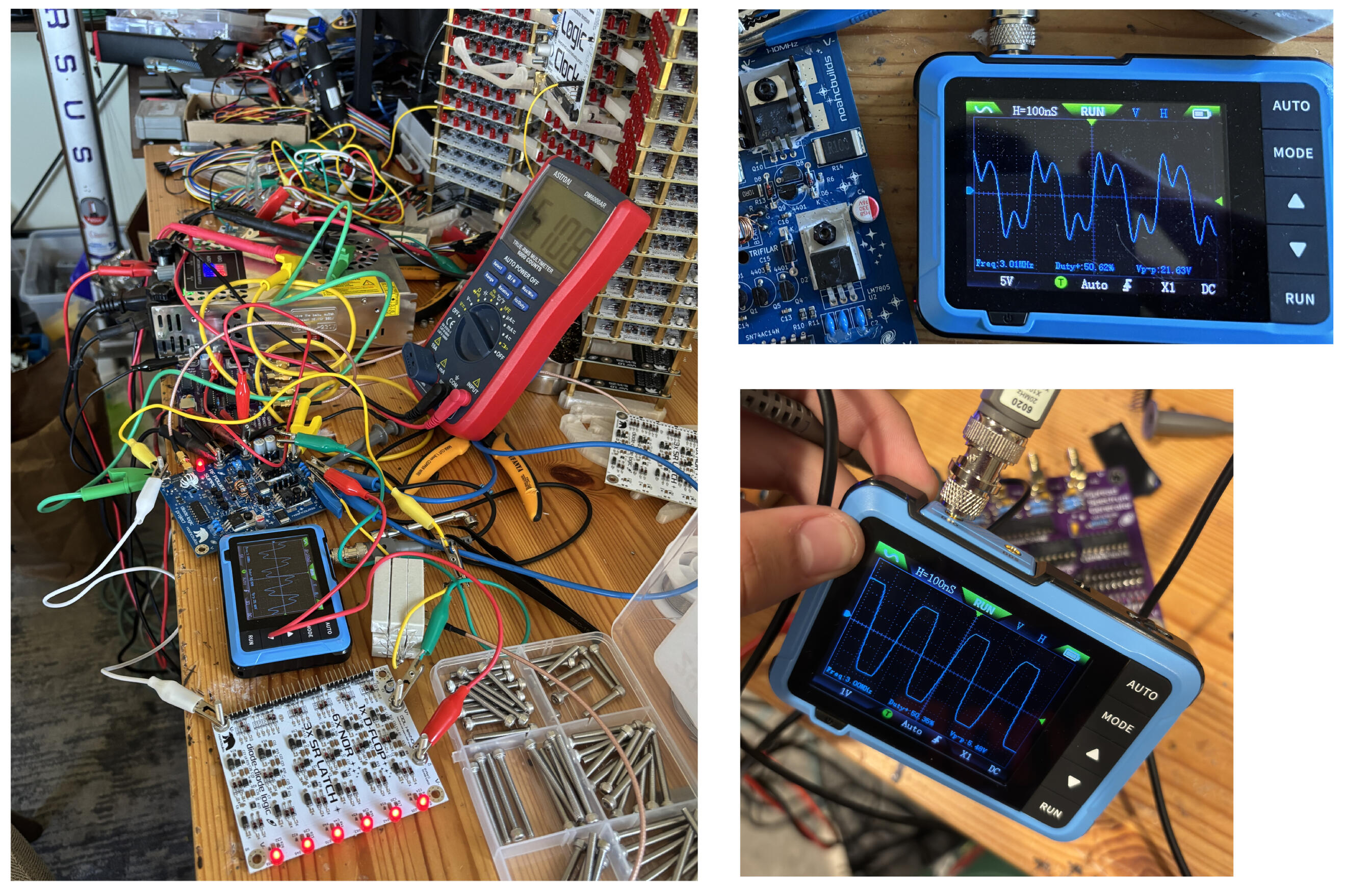
After finishing assembly of the signal generator and power supply, I needed to verify their performance. My school didn’t have an oscilloscope, so I bought a cheap handheld one off Amazon.Bottom right is the output of the signal generator, a clean 3 MHz 5.5Vp-p square wave. I fed this into the RF power supply, obtaining the upper right waveform with a 2.2 ohm dummy load (nine 20-ohm resistors in parallel, which I measured from my logic stack to be a good model of the load). The result contained 22V spikes and 12Vp-p averages. These spikes are within my MOSFETs’ 30V limit, although my oscilloscope’s 10 MHz sampling rate makes it hard to be sure. I’ve since decreased the amplitude of the ringing using a 220pF/10 ohm snubber (values suggested by Yapo that worked great for me). MOSFET temperature stabilized around a satisfactory 35C. Left picture is the verification of logic gates (all on because I left inputs floating).
~August to September 2025
5. Diode Clock Improvisations + Next Steps
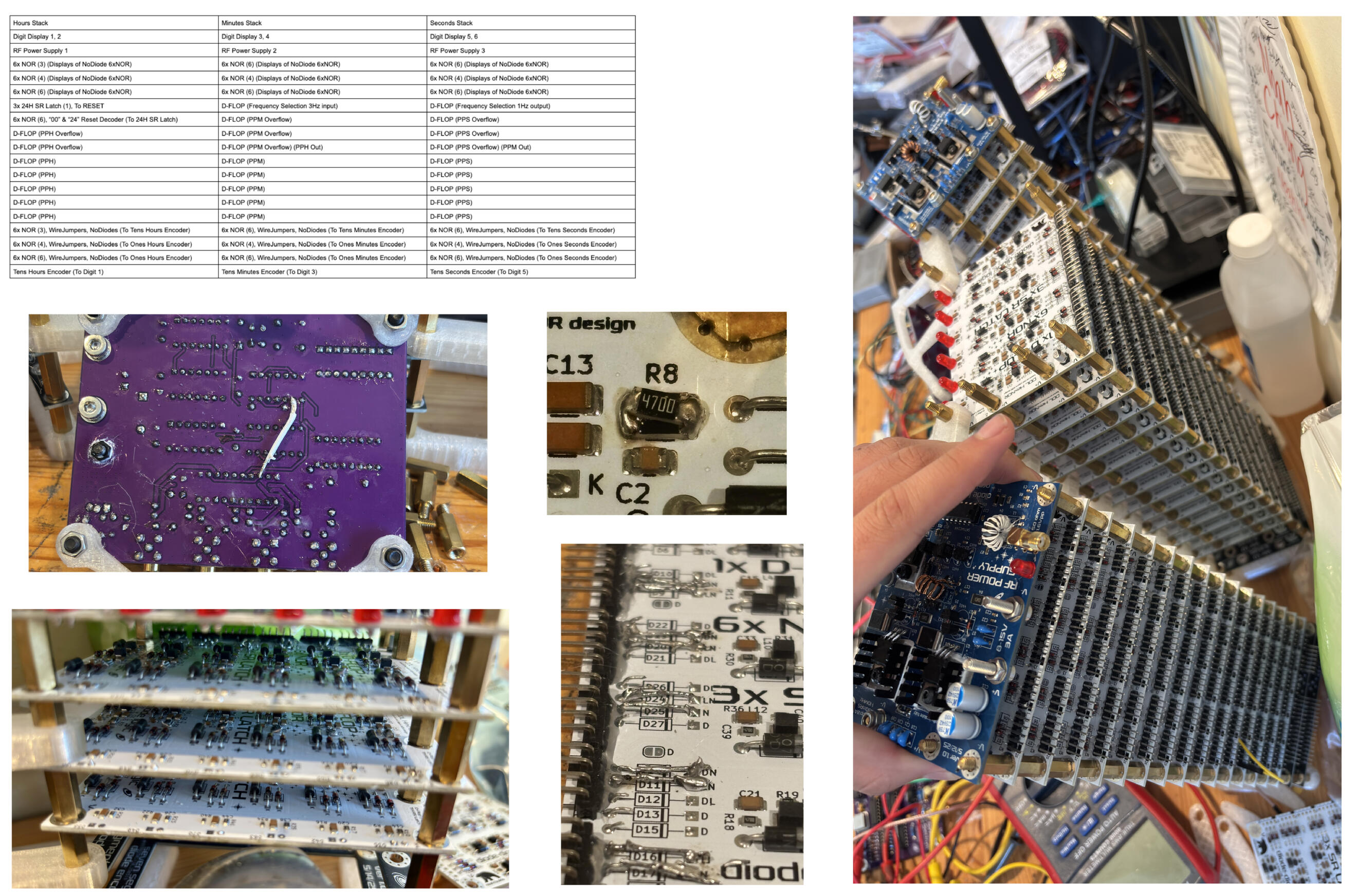
I still need to verify frequency divisor performance, build 7-segment displays, and wire everything up and test (via the pin headers on the back of the clock).I created my own logic board configuration guide to wire and stack 48 boards (top left). I removed redundant input protection diodes and LED outputs on the boards driving the diode encoders (bottom left and middle pictures). I increased output power for these boards as well by decreasing resistance between RF power and output (stacking another resistor on top of R8; middle picture). I debugged issues during assembly, like a missed connection on the purple signal generator, blown MOSFETS on the RF power supply, and faulty diodes on some of the logic boards.I now have a better understanding of discrete circuits, basic logic, and low MHz RF systems. I’m thankful to Yapo for putting his project on Hackaday, and I’m excited to continue building.
~September 2025 to Present